From a switch to CMOS logic
By How things work · myAudience
myAudience original rendered teaching illustration. Image: illustration, not a documentary photograph. · Operator-authored generated illustration; scientific concept model reviewed separately.
From a switch to CMOS logic
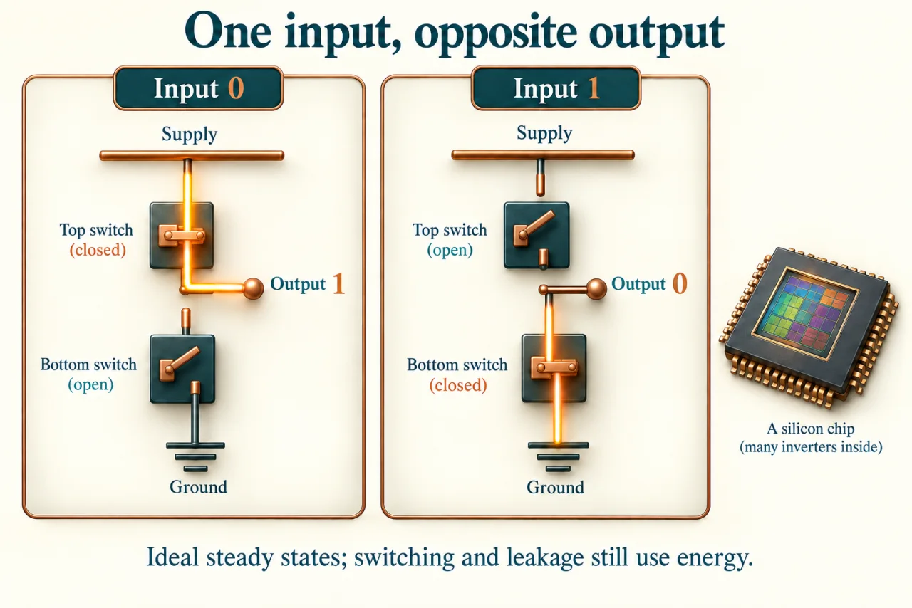
A digital 0 or 1 represents a range of electrical levels, not a tiny written numeral inside silicon. An inverter produces the opposite logical state. The illustration uses ideal switches so you can follow the connections without confusing a schematic with a fabricated transistor.
CMOS pairs complementary transistor types. In the elementary inverter model, a low input enables the pull-up path and disables the pull-down path: output becomes high. A high input reverses those states and output becomes low. Supply and ground are different rails; they must not be drawn as one uninterrupted wire.
A field-effect transistor controls conduction using a gate’s electric field. Manufacturing establishes material regions and device geometry; changing a logic input does not repeatedly dope the silicon. A switch drawing hides device physics, so it is a useful first model rather than a complete cross-section.
Ideal steady states avoid a continuous conducting path between the rails. Real devices have leakage, and switching charges or discharges capacitance. Consequently, low steady-state power does not mean a computer consumes no electricity. Noise margins and switching time also limit reliable operation.
CMOS logic is established commercial technology. Transistor geometry and fabrication differ between generations; this introductory model does not certify a device layout. Start with the logical relation, then ask what real electrical behaviour must be checked.
Discuss: should a designer prioritise lower electricity use or easier repair when neither option improves both? Explain who benefits, which evidence is missing and a reasonable alternative to your preferred choice.
Image: illustration, not a documentary photograph.
Worked example: Apply the inverter to the input sequence 0, 1, 1, 0.
For each stable input, output is the complementary logical state.
Replace 0 with 1 and 1 with 0, preserving sequence order.
Answer: Output sequence: 1, 0, 0, 1.
Check your understanding: Two ideal inverters are connected in series. What steady logical output follows an input of 1? Does this guarantee zero real power?
Answer: The first output is 0 and the second is 1. No: real leakage and switching energy still matter.
Why: Apply inversion twice. A truth table describes logical behaviour, not leakage, capacitance or timing.