How a wafer receives patterns
By How things work · myAudience
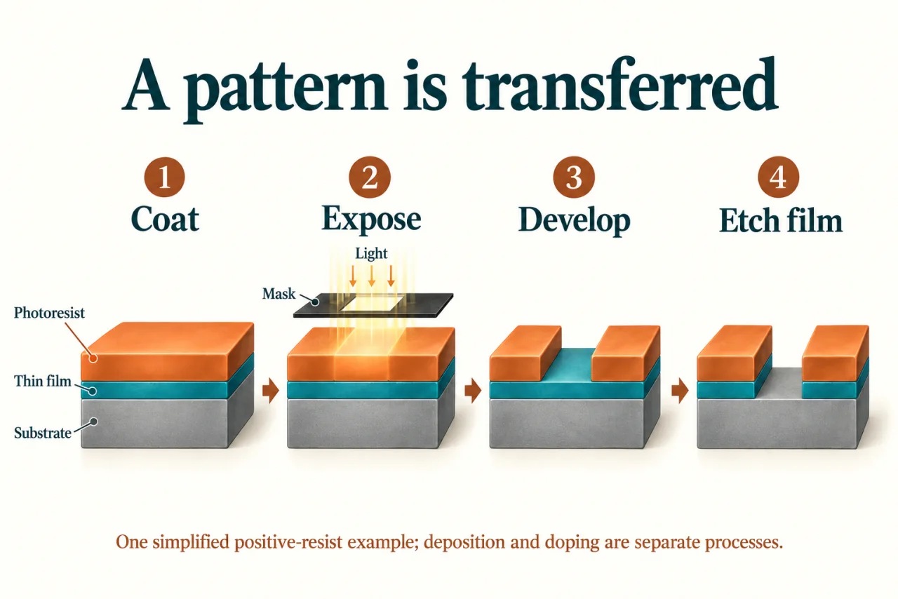
myAudience original rendered teaching illustration. Image: illustration, not a documentary photograph. · Operator-authored generated illustration; scientific concept model reviewed separately.
How a wafer receives patterns
A wafer receives many patterned material layers. Deposition adds a film; lithography determines where a later process acts. The illustrated cross-section represents one deliberately simplified layer, not the complete manufacture of a modern integrated circuit.
In this positive-resist example, a light-sensitive coating sits above the film. Exposure changes selected resist regions. Development removes those regions to create openings. The underlying film is still present immediately after development; this distinction prevents confusing resist processing with material etching.
An etch can then remove exposed film through the openings while protected regions remain. Other process flows use patterns for deposition or implantation, and negative resist behaves differently. Actual processes depend on material compatibility and selectivity; this lesson supplies no chemical recipe or operating settings.
Doping modifies semiconductor electrical properties through deliberately introduced impurities; implantation is one industrial method. Doping is distinct from drawing a pattern or switching a finished transistor. Success requires controlled processing and verification, not merely a beautiful image of tiny lines.
Lithography, deposition, etching and doping are established technologies. Their implementations vary, and leading-edge approaches continue to develop. Marketed process-node names are not interchangeable with exposure wavelength or every physical dimension on a chip.
Discuss: chip production offers useful products but needs energy, materials and controlled waste handling. What responsibilities should manufacturers and buyers share? Compare worker safety, regional resources and product lifetime without assuming innovation alone settles the trade-offs.
Image: illustration, not a documentary photograph.
Worked example: In a toy layer, positive resist protects 7 of 10 equal film regions after development. What fraction of film regions is exposed for the next etch?
Total regions = 10; protected regions = 7.
Open regions = 10 − 7 = 3.
Exposed fraction = 3 ÷ 10 = 0.30. Development itself has not removed the film.
Answer: 3 of 10 regions, or 30%, are exposed; the film remains until the subsequent film-removal process.
Check your understanding: After positive-resist development creates a central opening, is the underlying film necessarily already gone?
Answer: No. The opening is in the resist; a later selective process may remove or modify the exposed material.
Why: Resist development and pattern transfer into another material are different stages.